µTasker MCG (Multipurpose Clock Generator) Support - How to use the Kinetis MCG with ease
The Kinetis MCG (Multipurpose Clock Generator) allows a number of internal or external clock sources to be used to derive system and bus clocks from. The MCG varies between parts, some with PLL and FLL and some with only FLL but all follow a similar layout and similar rules for usage. The purpose of this discussion is to present the MCG in an easy to understand way and show how it can be worked with without the typical fear factor that can be induced by its formal documentation.
Note that the output from the FLL has higher jitter than that from the PLL and is not suitable as clock source for USB. For USB host mode, only the PLL should be used to derive its 48MHz clock from unless a dedicated USB clock signal is available. The same is true for USB device unless the Kinetis part includes IRC48M, which can be used to fulfil USB device specification requirements.
MCG Overview
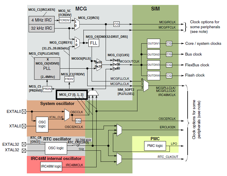
For this discussion the popular FRDM-K64F will be used. The K64 contains a full featured MCG, including PLL, FLL, RTC and an 48MHz R/C oscillator that can be used for USB device clocking as well as source for the system clock generation. A block diagram is shown below which is based on the diagram in the user's manual but with additional details about the registers involved which control its particuar configuration switches.
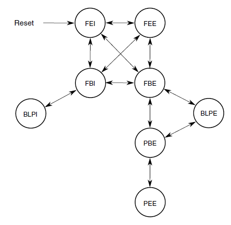
The second image is a copy of the MCG state transition diagram included in its formal description, which shows the possible states and also the allowed paths to move between them. What this diagram doesn't make clear on its own is what the states actually mean in terms of the practical configuration nor does it give details about why the transition between certain states is not allowed (or not possible) or give information about how the code involved can monitor successful transitions and avoid believing that it has completed one before really ready.
MCG FEI State
FEI is the first MCG state that exists automatically after every reset. It means FLL Enaged Internal and uses the slow 32kHz internal RC oscillator (32 kHz ICR) as source to the FLL (Frequency Locked Loop). The FLL defaults to a multiplication factor of 640 which means that the FLL output will be about 20.5MHz due to the fact that the 32 kHz ICR will be trimmed for this value in the factory. It does however have some deviation and temperature drift which makes it generally less accurate that a crystal source.
The PLL is disabled in the default state after reset.
The output of the FLL is switched to MCGOUTCLK, which then supplies the processor core and buses after optional dividers. The processor's clock is therefore about 20.5MHz out of reset and the default clock path is shown in the next diagram. The dividers in Kinetis devices generally defaut to divide by 1 since the initial clock speed is not higher than the maximum speed rating of any of the buses it clocks.
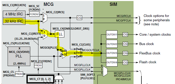
The FLL multiplication factor can be freely changed between its possible values (640, 732, 1280, 1464, 1920, 2197, 2560 and 2929)by adjusting the settings MCG_C4[DMX32] and MCG_C4[DRST_DRS] accordingly. Beware however that setting a high frequency (eg. about 93.7MHz with 2929) will result in a bus clock that is out of specification if the flash clock divider (OUTDIV4) is left at its default value of 1. It is therefore important to first program the dividers before programming the FLL multiplier to ensure that the destinations are not clocked too fast. In the case of the Flash clock being too fast it would probably cause the system to immediately fail.
MCG FBI and FBE States
FBI means FLL Bypassed Internal and means that the FLL is not used for the MCGOUTCLK but it is instead connected directly to an internal clock. FBE means FLL Bypassed External and means that MCGOUTCLK is connected diretly to an external clock (rather than an internal one). Both states are therefore similar in that the FLL is no longer involved, as is the PLL not involved.
The switching between the previous FEI and these two FBI and FBE states essentially involves adjusting the MCGOUTCLK switch to select where the MCGOUTCLK is taken from: FLL, internal clock or external clock as illustrated by the following diagrams:
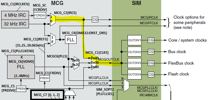
FBI selects an internal clock source
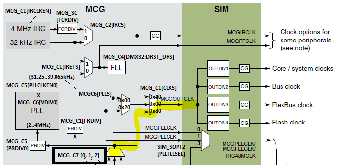
FBE selects an external clock source
To change the clock source the register field MSG_C1[CLKS] is used. If the internal clock source is selected it will be the 32kHz slow clock (32 kHz IRC) unless the fast IRC has been enabled and selected in MCG_C2[IRCS]. If an external clock source is selected, which one it actually is will depend on the configuration in MCG_C7 and whether the source is really available or not.
At this point it is worth noting three practical observations involving selecting the clock sources:
- When a clock source is selected it is often automatically enabled. For example, when the fast IRC were to be connected in MSG_C2 instead of the slow ICR and then selected as clock source for the FBI mode it is found that it is available although not explicitly enabled with MSCG_C1[IRCLKEN] - such details may be mentioned in the user's manual description of the particular clock involved.
- It is best not to select the slow IRC as a clock source since debuggers will tend to no longer operate correctly with such a slow speed!
- If the MCGOUTCLK is connected to a non-existent clock source, such as the RTC oscillator that is not enabled, the clock will not be switched to it and so the processor doesn't lose an input clock altogether. A value in the MCG_S (status) register reflects the clock that is connected and each time this switch is changed the corresponding value in the status register should be checked to be sure that the switch-over has been successful. Generally there can always be delays due to different registers being clocked by different clock domains that are not necessarily synchronised.
MCG BLPI and BLPE States
These state are essentially identical to the previous FBI and FBE states as far as clock operation is concerned. The difference is that the FLL (and PLL) are disabled by setting MCG_C2[LP] (not shown in the diagrams). By disabling the unused FLL (and PLL which will usually already be disabled if not explicity turned on) the power consumption can be optimised. The state transition diagram shows that BLPI is a dead-end state and this means just that the FLL should be re-enabled again to return to FBI and moving on to another state if ever needed.
MCG FEE State
The FEE (FLL Engaged External) state means that the FLL is being used as source for MCGCLKOUT whereby the FLL's input is not the slow internal clock but instead is derived from the external clock input selected by MCG_C7.
The switch controlling this state change from FEI is essentially MCG_C1[REFS] being changed from its default value of '1' [selecting the slow internal clock] to '0'.
Care should be taken to first select the external clock input to the FLL before switching because the FLL's input clock should be within the range 31.25..39.065kHz fo correct operation. This is achieved by ensuring that the source is availabe (eg. a RTC oscillator source may need to be first enabled), that this external clock source is selected in MCG_C7 and that the FLL's input divider MCG_C1[FRDIV] is set to divide it down to the correct frequency range.
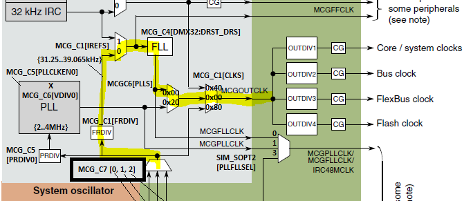
It is worth noting that the FLL's input selection is reflected in the MCG_S (status) register and if an external clock is selected that is not actually present the input will not switch - the value in the status register displays that the slow internal clock is still being used as source! Furthermore, if the input frequency range is invalid, eg. a fast external clock is connected without appropriate divisor setting, the FLL's input will indeed switch over to it but it will not actually be using the inappropriate value. The FLL will continue oscillating at its own resonance frequency since it can't lock to one defined by the source. If an external source is successfully selected but later removed (eg. by disabling the RTC clock) it doesn't cause the FLL to stop but instead it oscillates again it its own resonance frequence which keeps the system clocked, albeit with an inaccurate frequency.
Once the FEE state has been entered the FLL multiplication value can be changed as desired, whereby the bus divider values should always be written before increasing it to a frequency that could otherwise cause one of these clock to become out of specification.
For devices without PLL these MCG states as discussed above are already the complete set. This shows that the operation and control of FLL based MCG is in fact quite simple and not a lot can go wrong as long as the bus clock dividers are set to appropriate values before switching fast clocks to the MCGCLKOUT. It is recommended to avoid FBI from the slow internal clock due to the fact that debuggers tend to have problems operating from such a slow clock. Otherwise, the FLL is very robust and will continue oscillating even if attempts are made to use it without a clock source or with invalid source frequency. By monitoring the used state as reflected in the MCG_S (status) register it is easy to verify that the state changes were made as expected.
IRC48M Internal Oscillator and RTC Oscillator
Before completing with the MCG PLL base states and then giving some examples of real configurations it is worth mentioning the use of the IRC48M and RTC oscillators as external clock sources since there are a couple of potential pit-falls involved.
IRC48M Internal Oscillator
The IRC48M internal oscillator is available in various newer Kinetis devices and can be used as a clock source for USB device operation, in which case the clock is synchronised to the USB host's frame signal to obtain the required accuracy. In some devices there may exist a problem with enabling the IRC48M for use by the MCG due to the fact that it is only turned on from within the USB module; generally it is automatically enabed when selected as the MCG external clock. When using parts that require it to be selected in the USB module it means that the USB module needs to be clocked and the IRC48M enabled there before it can be selected for use at by the MCG. Furthermore, a USB reset at the USB module will stop the clock and potentially cause system failure. The µTasker configurations as shown later workaround this potential problem by enabling the USB module if it is detected that the clock cannot be selected as expected during initialisation and then by temporarily switching to an internal clocking state when the USB reset needs to be performed.
This subject is discussed in chapter 5 of Crystal-less USB operation on Kinetis MCUs - Application note AN4905 Rev. 1, 10/2014
RTC Oscillator
When the RTC oscillator is to be used by the MCG it is first necessary to enable it, although this may only need to be performed once when the RTC is battery backed-up and so usually operating continuously; the RTC oscillator is enabled with RTC_CR[OSCE]. In addition it is important to be aware of the fact that the 32.768 kHz output from the RTC oscillator is optional and can be disabled by setting RTC_CR[CLKO]. This setting is also retained across resets, and power cycles if the RTC has a battery backup and it is not to be excluded that the setting originally made in a system was with this output disabled. It is therefore advisable to always remove the RTC_CR[CLKO] bit before attempting to use the RTC oscillator as input to the MCG!
MCG PBE and PEE States
These states are only available when the MCG contains a PLL (Phase Locked Loop). The state PBE (PLL Bypassed External) is an intermediate state that is used to allow the PLL to be configured in and become stable before transitioning to PEE (PLL Engaged External) in which the PLL's output is being actively used as MCGOUTCLK.

PBE selects an external clock source for PLL and FLL and uses the same external clock input for system operation
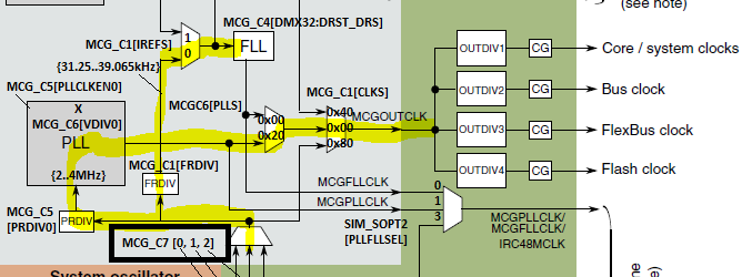
PEE switches the stable PLL output to MCGOUTCLK for use by the system
The PLL can only be referenced from an external clock source (that means external to the MCG since an available IRC48M is also valid as external source) and the transition to PLL use can only take place by moving via the FBE state.
From the MCG state transition diagram it is seen that PBE can also be entered from BLPE but this only means that MCG_C2[LP] has to be disabled since it is otherwise disabing both FLL and PLL.
Prerequisites for the PBE state are that the input clock is also switched to the FLL input and the PLL output path is selected as input to the MCG_C1[CLKS] switch otherwise the MCG_S (status) register will not confirm that the PLL has completed locking! Although the FLL is not actually used in the PBE/PEE states it is good practice to ensure that its input is still divided to its valid input frequency range.
Before completing the switch to PEE state the successful PBE state can be confirmed in that the MCG_S (status) register, which reflects that the PLL has successfully been selected instead of the FLL and that the PLL has achieved lock. The actual switch involves just changing MCG_C1[CLKS] from the external clock input to the PLL's output.
K61 MCG Comparison
The K61 has a MCG version supporting two external clocks and two PLLs. As comparison, the block diagram of this module is shown here, extended with some register details to aid in identifying its configuration control:
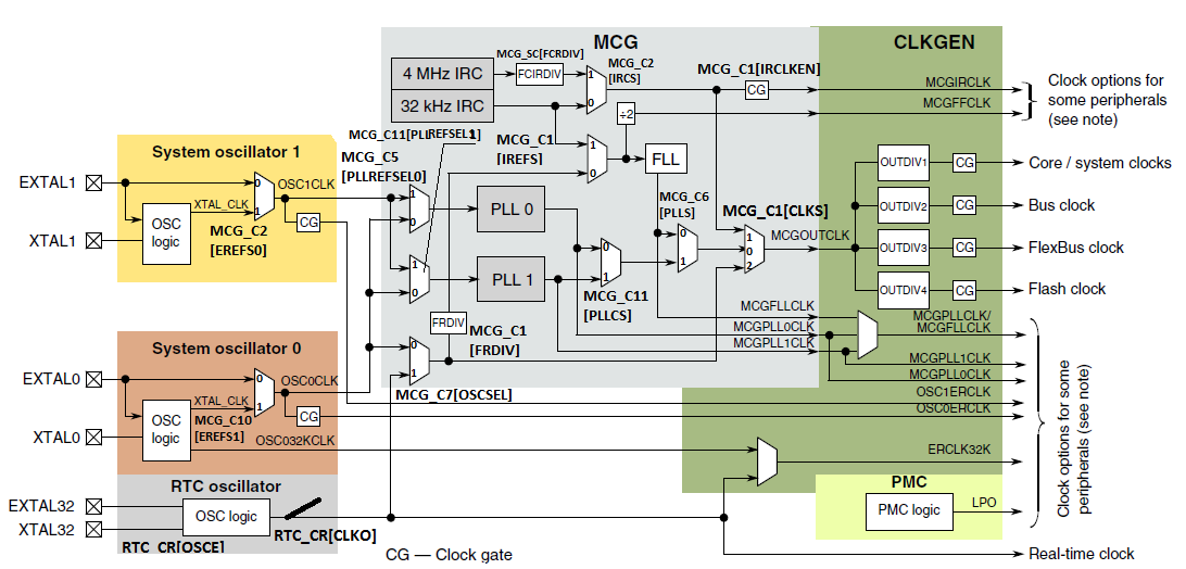
K61 MCG
Configuring Clock Speeds in the µTasker Project
The following is a set of clock options for the FRDM-K64F, allowing the user to choose the basic mode and then set specific frequencies. It specifically shows the PLL being used, referenced to the IRC48M oscillator, to generate a 120MHz system clock, 60MHz bus and 24MHz Flash clocks. The USB will use the IRC48M oscillator for its clock (USB_CRYSTAL_LESS) and so this configuration is suitable when no external clock is used, with restriction that Ethernet could not be operated.
  //#define RUN_FROM_DEFAULT_CLOCK                                       // default mode is FLL Engaged Internal - the 32kHz IRC is multiplied by FLL factor of 640 to obtain 22.5MHz nominal frequency (20MHz..25MHz)
  //#define RUN_FROM_HIRC                                                // clock directly from internal 48MHz RC clock
    #define RUN_FROM_HIRC_PLL                                            // use 48MHz RC clock as input to the PLL
  //#define RUN_FROM_HIRC_FLL                                            // use 48MHz RC clock as input to the FLL
  //#define RUN_FROM_RTC_FLL                                             // use 32.76kHz crystal clock as input to the FLL
    #if defined RUN_FROM_DEFAULT_CLOCK
      //#define FLL_FACTOR           2929                                // use FLL (factors available are 640, 732, 1280, 1464, 1920, 2197, 2560 and 2929)
        #define FLEX_CLOCK_DIVIDE    1                                   // approx. 22.5MHz
        #define FLASH_CLOCK_DIVIDE   1                                   // approx. 22.5MHz
        #define BUS_CLOCK_DIVIDE     1                                   // approx. 22.5MHz
    #elif defined RUN_FROM_HIRC                                          // use IRC48M internal oscillator directly (no PLL or FLL)
        #define FLEX_CLOCK_DIVIDE    2                                   // approx. 24MHz
        #define FLASH_CLOCK_DIVIDE   2                                   // approx. 24MHz
        #define BUS_CLOCK_DIVIDE     1                                   // approx. 48MHz
    #elif defined RUN_FROM_HIRC_FLL
        #define EXTERNAL_CLOCK       48000000                            // this is not really external but the IRC48MCLK is otherwise selected as if it were (Ethernet not possible!)
        #define _EXTERNAL_CLOCK      EXTERNAL_CLOCK
        #define FLL_FACTOR           2929                                // use FLL (factors available are 640, 732, 1280, 1464, 1920, 2197, 2560 and 2929)
        #define FLEX_CLOCK_DIVIDE    3                                   // 120/3 to give 40MHz
        #define FLASH_CLOCK_DIVIDE   5                                   // 120/5 to give 24MHz
    #elif defined RUN_FROM_RTC_FLL
        #define EXTERNAL_CLOCK       32768
        #define _EXTERNAL_CLOCK      EXTERNAL_CLOCK
        #define FLL_FACTOR           2929                                // use FLL (factors available are 640, 732, 1280, 1464, 1920, 2197, 2560 and 2929)
        #define FLEX_CLOCK_DIVIDE    3                                   // 96/2 to give 48MHz
        #define FLASH_CLOCK_DIVIDE   4                                   // 96/4 to give 24MHz
    #elif defined RUN_FROM_HIRC_PLL
        #define EXTERNAL_CLOCK       48000000                            // this is not really external but the IRC48MCLK is otherwise selected as if it were (Ethernet not possible!)
        #define _EXTERNAL_CLOCK      EXTERNAL_CLOCK
        #define CLOCK_DIV            20                                  // input must be divided to 2MHz..4MHz range (/1 to /24)
        #define CLOCK_MUL            50                                  // the PLL multiplication factor to achieve operating frequency of 120MHz (x24 to x55 possible)
        #define FLEX_CLOCK_DIVIDE    3                                   // 120/3 to give 40MHz
        #define FLASH_CLOCK_DIVIDE   5                                   // 120/5 to give 24MHz
    #else                                                                // run from external clock (typical configuration when Ethernet is required)
        #define EXTERNAL_CLOCK       50000000                            // this must be 50MHz in order to use Ethernet in RMII mode
        #define _EXTERNAL_CLOCK      EXTERNAL_CLOCK
        #define CLOCK_DIV            20                                  // input must be divided to 2MHz..4MHz range (/1 to /24)
        #define CLOCK_MUL            48                                  // the PLL multiplication factor to achieve operating frequency of 120MHz (x24 to x55 possible)
        #define FLEX_CLOCK_DIVIDE    3                                   // 120/3 to give 40MHz
        #define FLASH_CLOCK_DIVIDE   5                                   // 120/5 to give 24MHz
    #endif
    #define USB_CRYSTAL_LESS                                             // use 48MHz IRC as USB source (according to Freescale AN4905 - only possible in device mode)
  //#define USB_CLOCK_GENERATED_INTERNALLY                               // use USB clock from internal source rather than external pin - 120MHz is suitable from PLL
The main modes allow internal RC, IRC48M, RTC or external oscillator to be used as reference. The IRC48M can directly clock the system or be used as FLL or PLL reference. The internal 32 kHz can be used as FLL reference. The RTC can be used as FLL reference. If no specific mode defines are selected the default is to run from the external oscillator input (50MHz) and generate 120MHz with the PLL; this configuration would usually be used when Ethernet is required.
In each configuration case the FLL factor or the PLL input divider and multiplication factor can be defined. The divide value used by the system clock and buses can also be specified; when a system clock divide value is not given it will default to 1 and if the bus divide is not given it will default to 2. A non-specified FLL multiplcation value defaults to 640.
Should any invalid value be attempted, or any resulting frequency be out of specification, the build will generate an error informing of the bad value so that it can be corrected. Running the resulting code in the µTasker simulator will cause the actual vaues to be displayed for verification purposes. For example, the configuration above is displayed in the simulator as:

IRC48M Workaround
As noted previously there is a potential difficulty when using the IRC48M as clock source or reference to the PLL. This is because the early K64 devices enable the IRC48M in the USB module and the IRC48M is disabled when a USB reset is issued in that module. The result is that this can cause the system clock to fail if USB is used. Newer K64s don't have the issue since the IRC48M is enabled when it is selected as source to the MCG and so the USB reset also doesn't cause it to be stopped.
Unfortunately it is not known which devices have the problem and which not since this behaviour is not a device errata associated with a particulat chip mask. Therefore the µTasker framework implements an automatic workaround so that the code can be used on any device where the IRC48M is a source for the MCG and USB is in use.
The workaround operates by attempting to select the FBE state during initialisation and if it proves to be impossible (timeout) the USB module is enabled and the IRC48M enabled in it too. The fact that this had to be done is also saves as a varaible. When the USB initialisation takes place and the USB reset must be performed a temporary change to the FBI state from 4MHz internal RC oscillator is performed before the USB reset is issued. The IRC48M will be disabled in the process and afterward the original MCG state is again restored.
This allows USB to be used in any IRC48M based mode without needing to know which version of the K64 is being used. The side-effect of this workaround is however that the clocks will be temporarily slowed down during the USB reset which could effect any communication interfaces or timers in operation at that time. It is therefore recommended that the USB task be called early on before other such activity is started so that there is no risk of disturbance.
The workaround is not required when using the IRC48M source for the FLL since, as mentioned earlier in the document, the FLL operation is not disrupted when its input signal is temporarily removed. This doesn't however exclude a possible temporary frequency glitch when the USB reset is executed.
Conclusion
This discussion has presented the MCG in the Kinetis devices at a practical level showing that it is in fact simple and flexible to use when a few concepts are understood and a few potential pit-falls avoided. In addition, a workaround to a potential IRC48M problem in early K64 devices has been demonstrated, allowing all modes to be used successfully - irrespectively of the K64 version.
For specific questions and feedback please use the following forum entry: Kinetis MCG forumµTasker Kinetis MCG. Copyright (c) 2004..2021 M.J.Butcher Consulting