STM32F031 Clock Tree
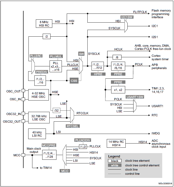
This blog entry discusses the clock tree as found in the STM32F031. The clock tree is one of the first things that one is involved with in such new developments. It is assumed that the tree itself is typical for such parts and so that the discussion is in fact of a more general nature than the part actually used as test vehicle.
Clocking in processors has developed a long way from a simple crystal oscillator used to drive most things at a single clock speed. There can be many sources and many choices and the subject has become one that can freighten even experienced developers. So much so that some may start by using some from of clock configuration tool supplied by the chip manufacturer. However the actual code involved is typically only a handful of lines and so basing project tool choice on something with a clock configuration tool just to save these few lines in developments that may run to hundreds of thousands of such lines seems to make much less sense than actually understanding the tree itself. And this is why this dicussion has been written...
Note that there is a (typical) clock module configuration as found in the Kinetis parts at Multipurpose Clock Generator.
We'll start with the clock tree diagram as found in the device's users manual and then elaborate on various details in order to get to know how understand what is going on and how to control it:

Clocking State out of Reset
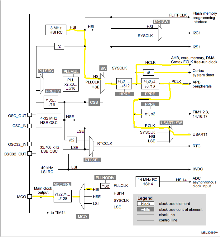
When the processor starts it has a default clocking configuration which allows it to start running code even without any external clock sources. Specifically it starts with a clock generated by the HSI (High-Speed Internal) RC oscillator. This has a fixed frequency of 8MHz +/- 1% at normal temperature but can drift by a further +/-1% over the normal temperature range [0..85°C] and up to a total of +4%/-3% over the range -40°C..+105°C. It takes between 1 and 2us to start up and is typically responsible for 80uA current consumption:
The following diagram shows how the HSI supplies basic clocking to the processor out of reset, whereby some of the control registers and relevant fields are also shown for clarity as to what is controlling this default configuration. It becomes immediately clear that the processor core is running at 8MHz, as are the various buses (AHB from HCLK and APB from PCLK). Peripherals could already be clocked from these sources and the system clock speed verified directly by routing it to the MCO output pin. The speed could also be indirectly verified by using the Cortex SYSTICK to generate interrupts based on its use of HCLK too. Basically, the default state would be suitable for a simple operating program without further adjustments at all!
The µTasker project target configuration #define USE_HSI_CLOCK and #define HCLK_DIVIDE 1 can be used to check this.
#define MCO_CONNECTED_TO_HSI additionally connects the frequency to the MCO output pin.
To optionally divide the clock output on the MCO pin, a define #define MCO_DIVIDE 128 can be used, where the value can be 1, 2, 4, 8, 16, 32, 64 or 128.

Blog in progress
Updates to follow...
µTasker STM32 Development. Copyright (c) 2004..2018 M.J.Butcher Consulting